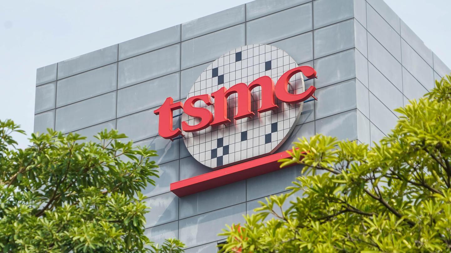
In 2026, Taiwan Semiconductor Manufacturing Company (TSMC) plans to start mass-producing its new manufacturing process, A16 (1.6nm), which was introduced at the 2024 North America Technology Symposium in California. The A16 technology promises to enhance logic density and chip performance by integrating advanced nanosheet transistors with backside power rail solutions.
Compared to the N2P process, A16 offers significant improvements such as an 8-10% increase in speed at the same operating voltage, a 15-20% reduction in power consumption at the same speed, and a density enhancement of up to 1.1 times to cater to data center products. TSMC stated that these benefits would enable them to provide high-performance computing solutions for various applications, including artificial intelligence, cloud computing, and edge computing.
During the symposium, TSMC also announced plans to invest $30 billion in R&D over the next three years to develop new technologies and manufacturing processes that would enable them to remain competitive in the global semiconductor industry. The company expects this investment to create around 8,000 new jobs in research and development positions across its facilities worldwide.
TSMC’s introduction of A16 marks a significant milestone in its ongoing efforts to develop advanced semiconductor technologies that meet the demands of modern computing applications. The company continues to be a leader in the global semiconductor industry and is committed to pushing the boundaries of innovation in order to provide its customers with cutting-edge solutions that drive growth and advancement across a wide range of industries.


:quality(75)/cloudfront-us-east-1.images.arcpublishing.com/elcomercio/YWR46Q5QCBCI5J3YRZ5VGAGZJ4.jpg)